Micro Capacitive Sensor
| Sponsors |
|
| Team Name | Micro Cap |
| Duration | Fall 2016 - Spring 2017 |
| Faculty Advisors |
|
| Graduate Advisor | |
| Students |
|
The goal of this project is to develop a printed circuit board (PCB) that utilizes capacitive sensors and an off-the-shelf capacitance-to-digital-converter (CDC) to detect and monitor micro entities. The monitoring process is an autonomous process that displays a plot of real-time capacitance values.
Problem Definition
Background
The counting and classifying of particles on the micrometer scale is expensive if automated and difficult if done using non-automated methods. The current system for particle monitoring is done by visually counting particles as they are passed under a microscope. An inexpensive automated counting and classification method for small particles needs to be created to lower the cost and increase the ease of use for this process.
Specifications
| Specifications | |||||
|---|---|---|---|---|---|
| General Requirements | Specific Requirements | Target Values | |||
| Resolution | The CDC chip needs to have very high resolution for detecting micro particles. | 16 - 24 bits | |||
| Sensor Plate Separation | The separation between the capacitive sensor plates needs to be extremely small. | In the range of 150 µm | |||
| PC Interface | This is necessary to see what the capacitance reading is from the CDC. | Very precise graph of capacitance vs. time | |||
| Firmware | A device (Arduino, FPGA, etc.) needs to be able to autonomously collect data from the sensor and CDC and interface with PC | Deliver useful capacitance data that is easily interpreted | |||
| PCB Design | PCB design should contain components to accurately sense micro-particles and convert capacitive values to a digital signal. | Single layer with multiple capacitive sensor design and CDC chips. | |||
Deliverables
- PCB designed with CDC chips and multiple capacitive sensor designs
- An easy to use graphing method that accurately displays capacitance vs time on a PC from the CDC chip
- A capacitive sensor design, or multiple designs, that successfully detects micro-particles
Project Learning
Capacitance can be very useful in sensing applications to detect the presence or proximity of various things. A very useful characteristic of capacitance is seen between electrodes (conductive material) when a dielectric is introduced between the electrodes, there is an associated capacitance change. The amount of capacitnace change is directly related to the make-up and permittivity of the material. This capacitance change can be measured on a sensor using a capacitance-to-digital converter (CDC) chip. By capacitance measurements of a sensor, a particle can be detected when there is a sudden jump in capacitance value. These sensors can be easily built on a PCB using exposed metal tracings.
The overall system layout will consist of a capacitive sensor that is read by the AD7746 capacitive to digital converter chip. This chip will be interfaced with a host Arduino microcontroller to autonomously gather data. The communication between the two utilizes I2C communication protocol depicted as SDA and SCL.
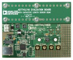
In the preliminary stages of system development we are using an off-the-shelf development board that hosts a microcontroller and AD7746 capacitance to digital converter. The evaluation board is able to use both the micro-controller and AD7746 CDC on board or optionally can be configured to allow use of these components separately. For this project the on board AD7746 CDC (evaluation CDC) can be bypassed by the micro-controller and communication can be established with the on PCB AD7746 CDC.
This will be used to test the PCB sensor design to ensure accurate functionality as well as CDC functionality. The development board or host micro-controller will interface with a PC to display capacitance measurements in a meaningful graphical interface. Another useful component for using the AD7746 evaluation board to trouble shoot system design is that it has graphical user interface (GUI) software to display and graph capacitance measurements.
Design Process
The AD7746 CDC chip is used on this project for its high resolution capability at 24 bits. High resolution is necessary in order to detect capacitance changes for the smallest micro-sized particles, which is possible for changes as small as 4aF. The CDC communicates the measurement data via I2C communication protocol to a host micro-controller system. The AD7746 development board was utilized to setup quick communication and display measurements for prototype sensor designs.
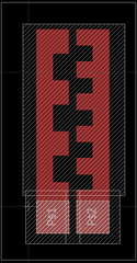
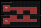
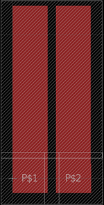
The capacitive sensors can be designed in a number of different configurations. The figure below shows a co-planer and inter-digital design. For the purpose of our project, the co-planer design was chosen so that we can utilize the "channel" down to the middle to fasten a microfluidic device.
Placing the microfluidic device over the capacitive sensor allows us to pump a sample over the sensor. As particles pass through over the sensor, the measured capacitance value will change.
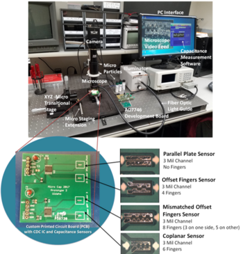
Utilizing the co-planer design template, four general sensor designs were considered. The designs consist of aligned fingers, offset fingers, mismatched offset fingers and parallel plate (no fingers). To further test how layout impacted sensitivity each of these designs parameters such as channel width, number of fingers, finger width and length and finger spacing could be altered. Varying these parameters may change the E-field between both plates and can cause certain sensor designs to be more sensitive and accurate than other designs.
The purpose of the testing process is to find which sensor design will be the most responsive to micro-particles passing through the "channel".
Three prototype PCB's were designed using EAGLE design software, each with a different layout style and several parameter variations. During the design process the CDC was placed as close as possible to the sensors to reduce the impact of parasitic capacitance from the metal routing. Other components necessary for the functionality of the PCB included decoupling capacitors for the power supply and two pull-up resistors for the SDA and SCL I2C bus lines. Lastly, pin heads were included to enable easy connection to micro-controller.
Testing Process
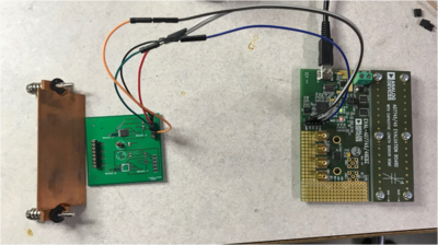
The sensors can be first tested using the microcontroller on the AD7746 Evaluation board. The picture shown displays this configuration where the evaluation board microcontroller interfaces with the prototype PCB and mounted CDC chip. Once a suitable design for the sensors is chosen, the next step will be to interface the on PCB AD7746 with our own microcontroller that will then display the capacitance values onto a monitor.
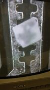
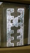
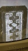
Initially, particles such as table salt (pictured), lemon pepper, and sodium bisulfate (pictured) were placed one particle at a time directly onto the sensor’s surface and the capacitance was read from the AD7746 development board software’s capacitance vs. time graph. The goal was to try and see if one sensor design stood out in terms of its ability to sense micro-sized particles. Since the particles varied in size greatly for some of the materials, this setup was deemed to be insufficient due to the lack of consistency. If the particle sizes vary, the particle size difference could have accounted for higher jumps in capacitance per particle added to each sensor.
Currently, an optical setup is being used that has multiple stages that are screwed down onto a stable tabletop. A tungsten needle is suspended over the printed circuit board that is directly under the microscope and the stages are used to move the needle horizontally and vertically. The tungsten needle is used to place particles on so that one particle can be used to test each sensor,
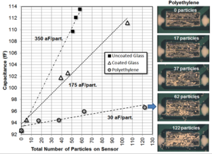
which makes the capacitance measurements more reliable. Clear nail polish was painted over the sensors in an attempt to try and protect the aluminum sensor fingers from particle debris, and testing is ongoing to see if it compromises the characteristics of the sensors too much to consider it as an option.
The next set of tests performed on prototype printed circuit boards used a micropipette to place even smaller polymer bead particles in the channels of the sensor designs. This way, the sensors were tested with particles that are of the size that is necessary for the eventual final medical counting system (around the size of white blood cells, etc.). Tests on the majority of sensors were inconclusive due to the extremely small size of the particles. This result prompted the need to revise the channel width of the sensors.
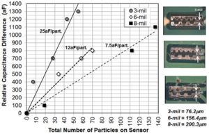
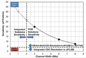
Using a 3 mil channel and micro particles on the scale of 60 to 90 micrometers, we graphed the corresponding capacitance increases for each channel width. As we suspected the smaller the channel size gave a larger capacitance jump. The 3 mil channel width PCB design again included all the same sensor layouts as the previous prototype to further test sensor physical layouts relation to sensitivity. Comparing fingered designs to the parallel plate (no fingers) design, the parallel plate showed a larger capacitance change with each additional test particle. From these results, the trend shows that with a smaller sensor channel width, the sensor sensitivity to capacitance change increases dramatically. Using an exponential best fit line on the data collected we could extrapolate sensitivities that one would expect to see if sensors were built using channel widths less than 3 mils. Unfortunatley, for a PCB based solution 2-3 mils is the minimum width for many PCB manufacturers to route metal tracings. Based on this data and constraints the application of this method calls for an integrated circuit solution.
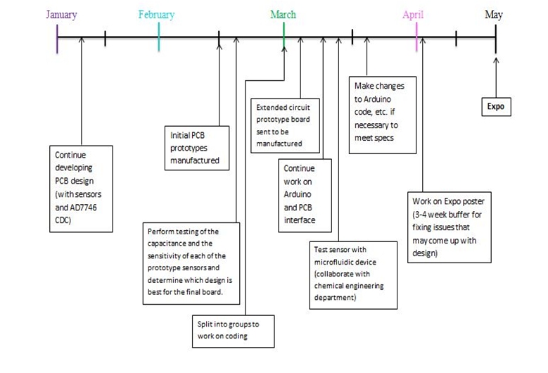
Spring Semester Timeline
The timeline for the spring semester will consist largely in testing the PCB design and debugging. The end of Fall semester is focused on the design of the prototype sensor design so that by mid Spring semester a final sensor can be manufactured and interfaced with the overall complete system.
