Solder Joint Reliability
| Solder Joint Reliability | |
|---|---|
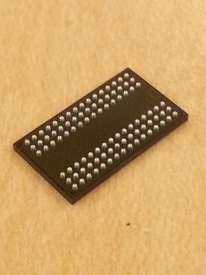
| An image of the test Ball Grid Array provided by Micron Technologies. These specimen will be sheared in the University's clean room after a set number of thermal cycles. | |
| Ball Grid Array | Two columns solder balls in a 3x16 arrangement. |
| Sponsors |
|
| Faculty Advisors |
|
| Timeline | Fall 2013 - Spring 2014 |
The solder joint reliability study will help indicate which solder type and surface finish combination provides the best mechanical strength to a system of electrical components after a series of repeated thermal shock cycles. This study will also create a finite element analysis model of solder joints in electrical components, and will model the effects of thermal cycles over time.
Problem Statement
The focus of the project will aim towards validating the solder joint bond strength at a point between a printed circuit board (PCB) and the electronic package that would be mounted to it. Using the known strengths of the materials, performing a thermal cycle testing sequence, and measuring the force required to break the solder joint bonds will predict which solder type performs the best in electronic packaging. This will allow future electronic packages to have a longer lifespan and will reduce costs to manufacturers.
Design Goals
The goal of our design project is to design a realistic finite element simulation of electrical components soldered using solder balls. This simulation will illustrate where fatigue and creep properties of the solder propagate cracks within solder joints that fix the electrical to the printed circuit board(PCB).
To help increase the accuracy of the finite element analysis our group will perform thermal cycling to compare the interaction effects of the 5 solder types and 4 surface finishes on bond strength of solder after a component endures similar conditions to Joint Electron Device Engineering Council (JEDEC) K-standard thermal cycling and is subjected to a shear strength test.
Design Specifications
To achieve a realistic model of electronic components soldered using solder balls we will establish material properties for the specific solder composition, and PCB surface finish used and enter our data into the computer simulation program Abaqus.
Background Research
| Solder Ball Cross Section | Description |
|---|---|
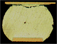
| This is a cross-sectional view of a solder ball after a fracture failure has propagated along its width. | |
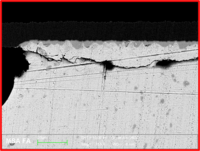
| This is a cross-sectional view of a solder joint's intermetallic bond after a fracture failure has propagated along its width. |
- As organic solder preservatives (OSP’s) are becoming an increasingly preferred choice in the electronic industry due to cost savings and more environmentally friendly compositions, it is crucial to component longevity to understand the interaction effects of lead-free solder and surface finish. With an increase in device complexity (including expansion into the mobile market), companies are concerned with solder joint reliability in manufacturing products that withstand thermal expansion and stress from physical impact.
Fracture propagation due to thermal expansion and mechanical shock occur in personal devices such as laptops, cell phones and other mobile electronic technology in the solder ball grid arrays (BGA’s).
- The difference between the thermal expansion coefficients of the ceramic printed circuit boards and the metal solder balls is the cause of fracture propagation and a major contributor to solder joint failure.
Experimental Design
With our project we are experimentally testing the interaction effects between differing solder compositions and printed circuit board surface finishes.
| Solder and Surface Finishes | Description |
|---|---|
| Table showing the five differing solder compositions and four surface finishes being tested. | |
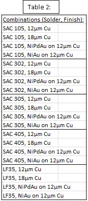
| Table showing the varying combinations of solder and surfaces finishes that we will use. Each solder and surface finish combination will be tested at varying numbers or levels of thermal shocking. |
Specimens will be tested according to JEDEC K-standard thermal cycling. Thermal temperature ranges is 0[C] -125[C] to an accuracy of +/-10[C]. Therefore, the thermal shock machine will be programmed to quickly shift between those 2 temperatures to stress the test specimens for 250 cycles. This thermal cycling will be representative of true JEDEC thermal cycling where the intermetallic layers between the solder pad and solder ball diffuse over time and create brittle sections across the contact surface. It is within these layers that crack propagation occurs and threatens the longevity of the component.
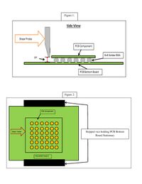
After the thermal shock test has been completed, each specimen will be subjected to a shear strength test to determine the reliability of the post-stressed solder joint combinations. The shear strength testing machine is capable of applying a maximum load of 10kgf (98.1N) to the edge of a component surface. To design the BGA size, a shear stress machine will operate near a loading of 5kgf which will allow the machine to operate in the middle range of performance. At this loading, a 6x6 BGA will fail near the target loading of 5kgf (within a small percent error).
| Experiment Components | Description |
|---|---|
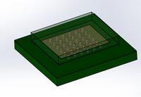
| Example CAD Image of the test specimen. | |
| Cross Section view of CAD test specimen. | |
| Shear probe setup used for measuring the shear force our electrical components can endure before experiencing critical fracture/shear failure. |
Experimentation Procedure
The goal of the experiment was to thermally shock solder joints under the JEDEK K standard condition. The JEDEK K standard condition outlines a hot soak temperature of 120°C and a cold soak temperature of 0°C. The soak time at temperature for our experiment we decided to be 5 minutes. This time was chosen because of time constraints and because as a group we thought it was enough time for the solder joint to come to temperature. This decision was confirmed to be appropriate by Micron and was within industry testing parameters. The ramp rate between temperatures was 2 minutes. Figure 5 shows a graphic of the thermal cycling of each component.
This is a thermal profile used for stressing our solder joints. The temperature will fluctuate from 0 to 125 degrees Celsius with a ramp rate of 2 minutes and a soak period of 5 minutes.
Thermally shocking the components in the thermal cycling machine would stress each joint. The testing procedure then became as follows:
- Select 3 random components
- Select 3 random rows for each component
- Shear off all 9 rows of solder balls, providing 54 data curves
- Put all components into the thermal cycle machine
- Thermally cycle all the components 100 times
- Repeat steps 1-5
The data taken from the XYZtec shear measurement unit is stored in a excel file. All the files for each round of thermal cycling were then compiled into one plot showing the shearing force with respect to the distance. The data was also analyzed to get a standard deviation to show the range of breaking force. A regression curve was then made to show the degradation of the solder ball joint with number of cycles. This information is crucial for the FEA model because it shows the strength of the solder joint with respect to the number of thermal cycles.
Experimentation Results
For the preliminary testing, the shearing tool on the XYZtec was insufficient. The tool was designed to shear off die and not solder balls. A new shearing tool was made to shear off one solder ball at a time. This greatly reduced the error in our data and made it more consistent. Once the new shear tool was made we started the testing procedure.
Using the data from the Shear Strength Plots for our specimens tested at 0 to 1000 cycles we were able to setup base conditions for a Finite Element Analysis model of the solder ball test specimen.
The development of the testing procedure and FEA model validated by data collected from testing was successful. With the data collected the FEA model accurately predicted failure of the solder joint at the same forces we saw with the data collection. However, the validity of the model could become better with more consistent data collection. Recommendations for future work include testing different combinations of solder types and surface coatings and a three dimensional FEA model of the electronic package.
Team Members
| Team Member | Backgroud |
|---|---|
| My name is Chadd Bergland and I'm a student studying Mechanical Engineering at the University of Idaho. My passion for engineering emerged after experiences with 3D design software and robotics. | |
| Joshua Carlson is from Boise Idaho. He started to become interested in engineering while growing up watching his father build and race cars. He later became an excellent high school student that excelled in science and math. He graduated from Meridian High School with college credits in Calculus and Chemistry. By this time he was also very knowledgeable about automobile repair and welding. This knowledge further increased his drive to become an engineer by making mechanical and thermal systems more efficient. Today he is expecting to graduate from the University of Idaho with a Bachelor of Science in Mechanical Engineering. The future is still unclear for him, but it is almost certain he will be in the engineering field making mechanical and thermal systems better all around. | |
| I am a mechanical engineering student at the University of Idaho, coming from the hometown of Boise Idaho. I am interested in computer aided design, and robotics programming. Outside of school I work as a Resident Assistant in the residence halls on campus. In my spare time I enjoy playing Ultimate Frisbee, knitting, and camping with friends. |
