DFIG Controller
| Team Into the Wind | |
| Team Name | Into the Wind |
| Duration | Spring 2020 - Fall 2020 |
| Faculty Adviser | Dr. Joe Law |
| Team Members |
|
The goal of this project is to design and implement a rotor side converter (RSC) that monitors a doubly-fed induction generators (DFIGs) torque, current and voltage output in order to command an input waveform that will stabilize the DFIG with the grid at 60Hz. The completion of this project will aid in the advancement of wind energy systems by allowing further research to be conducted on doubly-fed inductions generators.
Background[edit | edit source]
As the principal generator used in Type III wind energy conversion systems, the doubly fed induction generator (DFIG) is widely accepted in
today's wind energy industry. As society shifts toward renewable energy, these systems are becoming more prevalent. This brings an increasing need for research into how these systems interact with the grid. To achieve this end, the University of Idaho has created a wind turbine simulator which uses an AC induction motor to drive a DFIG at variable speeds and monitor power delivery and stability. In order to use this test bench, a full featured controller is needed operator the DFIG properly. That is the motivation for this project.
The DFIG is essentially a wound rotor induction generator
in which the rotor circuit can be controlled by external devices to achieve variable
speed operation. The stator of the generator is connected to the grid through a transformer,
whereas the rotor connection to the grid is done through power converters, harmonic
filters, and the transformer.
The stator of the generator delivers power from the wind turbine
to the grid. In the rotor, the power can be delivered from the rotor to the grid and vice versa through rotor-side converter
depending on rotor speed, and power factors. Two of the main components in the control system of the DFIG are the grid-side converter (GSC) and the rotor-side converter (RSC). The GSC is responsible for managing power delivery to the grid and generating a stable DC rail value from the grid to power the inverters. The RSC is responsible for controlling the power applied to the rotor in order to facilitate smooth, clean, and efficient power generation. The scope of this project is assembling and testing the components to create the RSC to be used with the wind turbine simulator test bench that the University of Idaho has built.
Deliverables[edit | edit source]
The focus for the first semester is understanding the systems involved and getting components ordered and tested. The process for this is the following:
- Learning to understand systems involved and components required
- Developing and verifying a design for the system using simulations
- Developing specifications and selecting hardware components based on design and verification
- Ordering components and testing individually to ensure expected function and specification compliance
Once hardware procurement and testing is completed, the plan for the second semester is the following:
- Perform component integration and subsystem tests
- Develop control code and test sub routines involved
- Complete any fabrication of custom components
- Mount components to power electronics stand
- Final integration and full scale tests
This outlines the process, and the final deliverables will be:
- A capable Microcontroller programmed with the required algorithms to run on the wind turbine simulator
- Power electronics components including Gate Driver, IGBTs, snubbers, rectifiers, etc.
- System connection components including any breakout boards and cables required to connect components
- Isolation components, in this case Optic Fiber links for noise immunity and isolation of high and low voltage components
- Sensors connected and tested in the final layout
Specifications and Constraints[edit | edit source]
Specifications for the project are listed below:
- Prototype must be modular
- Prototype must be robust
- Utilize startup and fail safe procedures in code
- Incorporate adequate isolation
Constraints of the RSC design were as follows:
- Integration must be designed to handle a DC bus voltage value up to 340V
- Must be able to stabilize a generator operating in a range of 0-60Hz with the grid (ie. 60Hz)
- Read sensor inputs and command the 3-phase inverter at a minimum frequency of 20kHz
Project Outline[edit | edit source]
Below you will find the schedule that was followed to complete this project. The gantt chart shown is a broad outline of the design steps taken. A detailed version can be found in the additional documents section of this page.
Design Evaluation and Verification[edit | edit source]
Space Vector Modulation and Controller[edit | edit source]
Evaluation of the Space Vector Modulation (SVM) algorithm began with studying and understanding the basic concept during the learning phase. Equations for our implementation of SVM were collected and used to create a more detailed simulation that accurately tested the implementation of SVM that will be used for the physical test bench. Essentially, this test consists of utilizing SVM in current control mode, determining the PWM scheme to use, devising an algorithm for causing the fewest switching events possible, and finally testing how this interacts with an inductive load.
To test active current control, a PI controller was implemented in the simulation. The three phase current measured in the load was converted to Direct-Quadrature (dq) axis rotating reference frame in order to have stable value (i.e. current values are essentially constants), then it is not difficult to implement a PI controller that can maintain the currents very close to the command, even as the command changes. Next, we decided to use center aligned PWM with three channels (one for each phase leg) with six outputs (three positive and three negative or complementary). This makes applying the derived vector straightforward and provides protection for power electronics by maintaining the switch configuration in one of the eight possible safe states. Using center aligned PWM also naturally allows us to reduce the number of switching events (by ensuring that all states are not toggled to on/off at the beginning of each cycle) while also staying in each state for the correct amount of time. In each cycle, the SVM algorithm generates a time for each of three states. These consist of two adjacent non zero states and a zero state (the remaining time for a cycle). There are two zero states where there is no net current flow through the balanced three phase load (i.e. states 000 and 111). By properly utilizing these zero states, we are able to ensure that only one phase leg changes state at a time.
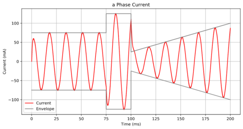
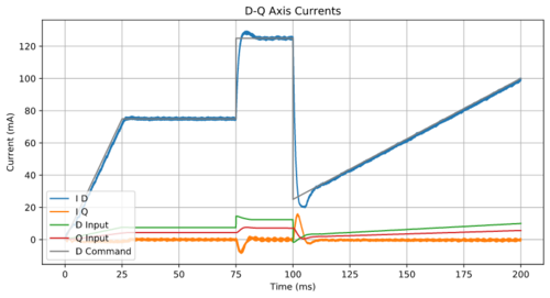
With the PWM waveform generated, the simulation tests how this waveform would interact with an inductive load. To test this, we generate a transfer function for each phase of the load. We feed the voltage waveform generated by PWM through the transfer function in order to obtain a current estimate. This is done in each phase and is used to calculate the overall current in the dq rotating reference. This overall current is compared to the command to generate an error function which is used by the PI controller to actively adjust the command to control the current phase and magnitude. The results of the simulation are shown in the following figures.
After completing this simulation and gaining a reasonable understanding of the control system in general, it was possible to develop a list of requirements for the microcontroller to use in the project. The notable requirements are:
- Clock speed >100 MHz with PWM capable timers at >20 MHz in order to provide at least 9 bits of resolution at a fast switching frequency of 40 KHz (for standard PWM). *Note: 9 bits = 512 steps = max 0.66 V/step @ 340 V DC rail
- Advanced PWM capability including 6 channels (automatic 3-phase complementary a bonus) and center aligned mode.
- At least 6 simultaneous ADC channels with at least 12 bits of resolution
- Various communications protocols including I2C, SPI, CAN for interfacing with other modules
- Hardware math accelerators such as FPUs and MACs (usable without assembly wrappers is a bonus)
- Free IDE with plentiful documentation, code samples, libraries, and developer community
Power Electronics[edit | edit source]
The first step in the design evaluation process from the power electronic side of this project was to investigate the integration of the gate driver with the IGBTs. Research during this portion led us to two possible solutions for our design:
- implementing a three-phase gate driver with a six pack IGBT module
- implementing a three-phase gate driver with three two pack IGBT modules
If we were to utilize the first proposal the end design would have been more compact and would demonstrate higher performance. However, this idea also required a large portion of our budget to be placed towards buying equipment in order to mount the six pack IGBT module since it was a newer IGBT housing design. After consultation with our client the second solution was chosen for implementation due to costs, as well as keeping the final design modular. Along with the choice of implementing a three-phase gate driver with three two pack IGBT modules we also decided to purchase a high-side low-side gate driver in order to conduct small scale tests without risking damaging our three-phase gate driver.
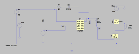
After deciding on a model for gate drivers and IGBTs, simulation models for each device were able to be plugged into LTSpice simulations to verify our design before purchasing the components. Simulations conducted to validate our choices consisted of creating a single leg circuit and H-bridge circuit. The schematics used for these tests can be seen below:
Following research involved with the gate driver and IGBTs the next power electronics design revolved around incorporating the protection circuits and components. Protection for our design focused on two main topics: snubbers and MOVs. Snubber circuits were chosen in order to minimize the switching losses of our design while also protecting the IGBTs by minimizing the losses of each IGBT and therefore reducing heat transfer in the devices making the design more robust. The calculations seen below were used to determine the snubber capacitor and resistor values and the inductor value was chosen by referencing the principle of duality:
After calculating values the components were integrated into the original single leg Spice simulation to verify functionality and many reiterations were conducted after making changes to the inductor, capacitor, and resistor values. Simulations were ran until the voltage and current waveforms of the IGBT produced results displaying acceptable power losses along with current and voltage values well within the rating of the IGBT. Results from these tests showing the turn on and turn off characteristics can be seen below:
These tests resulted in the following finalized values for the snubber circuit:
- 50 Ohm resistors
- 1.2uH inductors<>
- .12uF capacitors
Alongside snubbers the other means of protection mentioned were the use of MOVs. MOVs were utilized as an extra layer of protection for the IGBTs in order to act as a path for current to flow if an unexpected spike were to occur. MOVs were selected based on the following parameters:
- Varistor voltage
- Continuous rms voltage
- Peak pulse current
The last two design components to be simulated for verification and understanding purposes were the three-phase inverter and the high voltage (HV) side power supply. An ideal circuit had to be implemented for the three-phase inverter in order for Spice to run in a timely manner due to the complexity of timing involved with the fully integrated design of the three-phase inverter. A schematic for the ideal three-phase inverter and its results can be seen below:
This simulation served as a means of understanding and having a visual representation of the end goal of this project and reference for tests in the lab.
Concluding the power electronics verification stage was a simulation to validate component selection for the HV power supply which consisted of:
- 120:12V transformer
- Full wave rectifier and its smoothing capacitors
- Two DC-DC converters
A schematic and results for the Spice simulation regarding the HV power supply can be seen below:
This simulation utilizes a voltage source to represent the voltage seen from the output of the 120:12V transformer and a current source depicting the total load current being drawn by the devices that it will be supplying power to.
Hardware Procurement[edit | edit source]
Various new pieces of hardware were required for satisfying the requirements of the project and to replace out of date or broken components from previous projects. This section details the hardware we picked, gives some of the critical specifications and the justification for choosing the specific module. Information detailing the smaller components utilized for the snubbers, full wave rectifier, noise filtration, and all other components has been left out to avoid clutter. If interested in viewing information regarding these components the datasheets for all of the components can be found in our portfolio.
Power Electronics[edit | edit source]
IGBTs[edit | edit source]
The final choice for IGBT was the FF200R06KE3 by Infineon.
The main parameters of the FF200R06KE3 that led to our choice were:
- its 600V collector-emitter voltage
- its low collector-emitter saturation voltage of 1.6V
- its 200A continuous collector current
- its timing parameters that corresponded to a dead time of approximately 1us
Gate Driver[edit | edit source]
The final choice for gate drivers were the 6EDL04I06PT by Infineon as the three-phase gate driver and the IR2101(S) by Infineon as the high-side and low-side (single phase) gate driver.
Main features of the three-phase gate driver that dictated our choice were:
- its voltage rating of 620V
- its capability of separate control for each driver
- its extra built-in protection and signal interlocking capability of every phase.
The choice of the IR2101 stemmed from our decision of the three-phase gate driver we chose. Since it would be serving as a research tool to familiarize ourselves with the gate driver and IGBT interactions of our design, the IR2101 was chosen due to its similarities to Infineon's 6EDL04I06PT gate driver.
Controller and Sensors[edit | edit source]
Microcontroller[edit | edit source]
| The microcontroller we picked for the project is the STM32G474E-EVAL board from ST Microelectronics. This evaluation board is meant for motor control applications as well as a range of other tasks. The versatility of this board is wide, but that is also one of its weaknesses as it relates to this project. Because it contains so many peripherals connected in various ways to the package, the pinouts on the board are not exactly advantageous for this project. Luckily, the board contains extension headers which give access to nearly all IO pins on the package. Using a custom breakout adapter, the board can be set up to work perfectly for this project without sacrificing the versatility by modifying the board itself or getting a differently configured board. |
Notable Features[edit | edit source]
- 32-bit ARM Cortex-M4 CPU (@170MHz)
- Includes FPU, Real-time Accelerator, hardware trigonometric function evaluation
- 512KB flash memory, 96KB SRAM
- 107 GPIO pins
- Various types of high resolution timers
- 6 channel automatic complementary PWM generation with center aligned mode, emergency stop, automatic dead time insertion
- Free IDE with various examples demonstrating peripherals usage, standard debug features
- CAN, I2C, UART, SPI communication interfaces
Unfortunately, this microcontroller only contains 5 ADCs that can be run simultaneously.
This board can also be used with Simulink to run and debug Simulink models and convert them directly C/C++ code that can run independently on the microcontroller. This requires STM32CubeIDE/STM32CubeMX along with MATLAB + Simulink with MATLAB Coder, Simulink Coder, and Embedded Coder. However, we tried to go this route and found that Embedded Coder plugin is not available for purchase on a personal/student/home license and would have to be purchased through the University to be used. If successful though, this would offer an excellent option for researchers to skip the coding and use Simulink models that can be tested in simulation and Processor-in-Loop (PIL) beforehand to program the microcontroller.
ADC Module[edit | edit source]
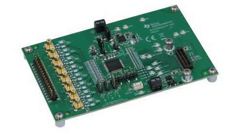
| The external ADC module we picked is the ADS8588EVM-PDK from Texas Instruments. This high ADC evaluation module contains the Texas Instruments ADS8588 ADC which contains 8 simultaneous ADCs, communicates over a fast parallel interface and has the ability to also communicate over serial interface for maximum versatility. Other options were considered such as using the on board ADCs on the microcontroller, as in using 4 in simultaneous mode with the remaining one operating in multi channel mode. While this may have worked for 6 channels, it is not a very clean and modular solution. Other cheaper modules were evaluated but they use only a serial interface which ends up being much too slow to deliver data at the rate the datasheet claims the ADC can sample. Finally, having a seperate ADC module allows the ADC to be connected very near to where the analog signals are measured thus reducing noise in analog measurements. Then, the digital signals can be sent over the relatively larger distance and are less likely to be corrupted by electrical noise. Thus this ADC was our final choice. |
Notable Features[edit | edit source]
- 8 simultaneous sampling channels at up to 200Ksps/channel
- True Bipolar inputs support +-5V or +-10V depending on configuration
- High input impedance to allow direct connection to sensors and devices without buffers
- Fast parallel interface
- Evaluation module includes standard breadboard header for connecting to analog inputs as well as SMB connectors
- Precision Host Interface (PHI) module adapts board to connect to PC computer and run free Texas Instruments software to test the module. Software is available at the product page.
Along with this ADC module, a Samtec breakout adapter was purchased to convert the compact Samtec header on the evaluation module to standard sized pins (2.54 mm pitch) to allow direct connection, testing, and prototyping with the microcontroller without making another custom PCB with the Samtec connector.
Isolation[edit | edit source]
Transmitters & Receivers[edit | edit source]
The transmitters and receivers chosen were the AFBR-2624Z models by Broadcom Limited. These were chosen since they were able to transmit signals at a rate up to 50MBd and utilized TTL input logic.
Fiber Optic Cables[edit | edit source]
The fiber optic cables chosen were the IF 1L1M-0-5 model produced by Industrial Fiber Optics and were chosen because they were cheap and compatible with the transmitters and receivers we went with.
Implementation and Testing[edit | edit source]
Gate Driver and IGBT[edit | edit source]
Testing the high-side low-side gate driver was first performed in complete isolation using power supplies to command input signals of the gate driver and observe the output ports. Once configurations of the gate driver had been reassured by test results, the gate driver was tested along with the IGBT module by creating a RC charge circuit consisting of:
- the gate driver
- the IGBT module
- a RC load
- a waveform generator to command the inputs of the gate driver
- a 6V source used to charge the circuit
A schematic for this setup and actual circuit build can be seen below:
Results for these tests will be found in our portfolio (these results are in the format of a video showing the charge and discharge of the capacitor). In the test the waveform generator was first utilized to create the input signals but later on the microcontroller was used to send the signals through our optic links. In both tests two square waveforms (inverse of each other) with a frequency of 22 Hz were sent as input signals allowing for full charge and discharge of the circuit.
High Voltage Power Supply[edit | edit source]
The HV power supply testing aimed to verify the integration of the components that made up the design (the transformer, rectifier, and DC-DC converters). This test first observed the input voltage the transformer saw from the wall outlet and what voltage level it was stepping the input down to. After observing these values the transformer output was connected to the rectifier circuit to observe the rectified voltage value. Since this test produced results that contradicted the values proposed by the transformer datasheet, the output from the full wave rectifier was not compatible with the input voltage range of the DC-DC converters selected.
To continue this test to verify component compatibility alterations to the circuit had to be performed. These alterations included implementing a voltage divider into the rectifier circuit by using a 1.5kOhm and 4.7kOhm resistor to bring down the rectified voltage to 14.85V. With the rectified voltage now within the DC-DC converters rated voltage range of 9-18V the integration of the transformer, full wave rectifier and DC-DC converters was tested and the desired outputs of 3.3V and 5V from the DC-DC converters was verified.
Software Testing[edit | edit source]
With the SVM and PWM schemes implemented and tested in the simulation, we moved on to implementing and testing them on the microcontroller. Converting the simulation to C code to be run on the microcontroller was fairly straightforward, although some optimizations may be required if the final control loop is found to be running too slowly. For testing the SVM and PWM however, the algorithm ran plenty fast. The basic test algorithm runs a loop in which each iteration takes the command current in the dq space and the dq reference frame angle and uses this information to run the SVM and generate the PWM switch times. These are then applied to the three channels which are output on the motor control header pins on the microcontroller as 3.3V digital signals. To test that generated signals are correct, they were inspected via an oscilloscope. It may seem somewhat difficult to determine if the signal is exactly correct through an oscilloscope since it progresses so quickly (60 Hz sine wave with PWM pulses at 20KHz) however, using a few techniques it is not too difficult to verify that the output is reasonable. One of the more obvious steps is to simply slow down the generated sine wave command to something like 1 Hz which will allow easy monitoring of the progression of the pulse widths. Once it is verified that the pulses widths are following a sinusoidal progression on all three channels, we next verify the proper shape waveforms for all channels. It should not be too hard to inspect a few examples of all three positive channels together to ensure the proper center aligned waveform is displayed with all channels progressing in a sinusoidal fashion with 120 degrees separation. Finally, confirm that each positive and negative channel pair are complementary with the proper dead time inserted.
PWM Small Scale Testing[edit | edit source]
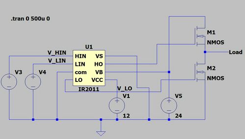
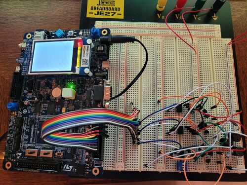
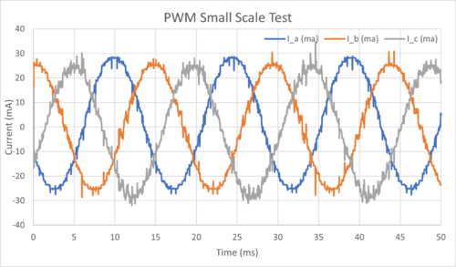
After verifying to the extent possible with the oscilloscope, a circuit was constructed to better test the outputs. The circuit consisted of three Infineon IR2011 (single phase high/low side) gate drivers connected to the logic outputs of the microcontroller with the gate driver outputs driving the gates of six 60V NMOS power MOSFETs which stand in for the IGBTs that will be used in the final design. There are three high side MOSFETs and three for the low side, connected in the typical 3-phase inverter topology (see figure Basic 3-Phase Inverter Topology in Appendix D and Appendix H). Connected to the floating node on each leg of the inverter is the corresponding inductive load for that phase leg. In the case of the PWM small scale test performed for this project, both the simulation and the physical test used an R-L load consisting of a 100 Ohm resistor along with a 150 mH inductor. This provided a small and stable current at 60 Hz and allowed the current in each phase to be measured via the voltage across the resistor. A single leg gate driver and MOSFET connection is shown in the following LTSpice schematic. Also shown are the real circuit on a breadboard connected to the microcontroller running the SVM algorithm, and the measured current obtained using this setup.
|
One notable issue with the physical testing is that the microcontroller had to be physically modified to connect the PWM outputs to the motor control header pins (modifications required are bridging solder pads and removing components, these steps are listed in the microcontroller user manual). Another option is using the extension headers provided, as all signals are accessible from these headers, however the pin spacing is a non standard size and difficult to connect to with the standard jumpers. The next step for the small scale testing is to add in feedback via an ADC module to test closed loop current control. This was not finished as the onboard ADC modules would work but do not have accessible pins without board modifications or a custom breakout board/adapter for the extension headers, and the external ADC module that was ordered to connect to the sensors on the power cart on have a custom PCB breakout board for the microcontroller extension headers. After this, the field oriented control algorithm can be implemented and validated before integration testing with the higher voltage components. |
Optic Links[edit | edit source]
Given the importance of isolation the optic link components (transmitters, receivers, and fiber optics) were the first components to be tested. All that was needed to conduct this test was our microcontroller and two breadboards. This test was performed to observe functionality of the microcontroller and the optic links and compare the signal delay created from the optic links in a test environment to the delay listed for the devices in the datasheet. Following these tests and the manufacturing of the transmitter/receiver perfboards tests of the perfboards created were also complete in a similar manner. The test setup for the original test along with an image of the perfboards used in the following test can be viewed below:
Tests on the perfboards were conducted to ensure components were properly configured and soldered onto the perfboards. Results for these tests can be seen below:
Final Design[edit | edit source]
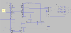
System design originated as a Spice schematic and evolved during the building phase of the project. A finalized Spice schematic displaying connections for our final design can be seen below:
This schematic includes all equipment except for the sensors required to measure outputs from the wind turbine simulation machine.
In the schematic you will find:
- a symbol depicting the microcontroller with I/O ports
- passive components used for noise filtration for the transmitters
- the transmitters
- leads between the transmitters and receivers representing the fiber optic cables
- the receivers with their corresponding noise filtration components
- transmitters and receivers utilized for sending signals to control the IGBTs are located in the top portion while the two sets of optic links below are used for viewing the fault pin and commanding the enable pin of the gate driver
- transmitters and receivers utilized for sending signals to control the IGBTs are located in the top portion while the two sets of optic links below are used for viewing the fault pin and commanding the enable pin of the gate driver
The aforementioned components make up the low voltage (LV) side of the RSC design as well as the link to the high voltage (HV) side.
The rest of the schematic relates to the HV side of the RSC and includes:
- the HV power supply
- the gate driver
- the external components needed for the gate drivers function
- the IGBTs
- the heatsink
- the snubber components
- the location of the DC rails (+/-)
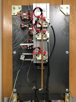
Following the conceptual design layout of the RSC was the actual stand configuration and manufacturing process. An image showing the current stand configuration can be seen below:
In this image you will see that all receivers/transmitter were mounted to the stand via mount rails that attach to the heatsink and are located at the top portion of the stand. The transmitters/receiver sending the signals to the ones viewed are directly across from the ones viewed on the LV side of the stand. Further investigation of this image shows the mounting of the HV power supply perfboard and the transformer (located below the receivers and mounted in the same manner as the receivers) along with the location for the gate driver PCB which is also mounted on the heatsink, but in front of the previously mentioned subsystems. The layout described allows for easy interconnection of each device. The last components viewable in the image above are the IGBT modules, the snubber components and the negative rail with leads to the output ports of the RSC. Snubber components have been mounted directly to the negative rail and IGBT nodes to improve performance.
Future work[edit | edit source]
Future work needed to be completed for this project can be broken down into five topics, all of which have been partially completed but have some advancements needing to be implemented. These topics include PCB fabrication, high voltage side stand configuration, low voltage side stand configuration, coding, and system testing.
Tasks involved with the future work associated with PCB fabrication are as follows:
- PCB printing (gerber files provided)
- RCin port capacitor chosen
- ITrip port capacitor chosen
- ITrip port resistor chosen
The PCB board needing to be printed is for the gate driver and its external components utilized in the protection abilities that the gate driver device provides.
Steps needing to be completed to finish the high voltage side of the prototype include:
- Mounting the PCB and making gate driver connections (mounting hardware already in place)
- Twist soldering snubber components (snubber components already in place)
- Drilling extra holes on the heatsink for proper IGBT mounting
- Mounting the positive rail
- Connecting power supply outputs to the optics and gate driver(devices already mounted in a layout that provides easy interconnections to be made)
Low voltage side stand configurations tasks needing to be completed are:
- Mounting uC and making connections to the optics and sensors
- Creating the breakout boards that will aid in the connection process of the uC (schematics for these boards are provided)
In terms of coding the only task needing to be completed is to write and verify the field oriented control algorithm.
Following these tasks the last item involved with future work is to run tests utilizing the wind turbine simulator and the RSC design. It is advised to run a few small scale tests verifying system integration before performing tests with the wind turbine simulator.
Team Members[edit | edit source]
|
Mason Ulrich | |
|
Mason Taylor | |
| Keegan Miley-Hunter Major: Electrical Engineering |
Additional Documentation[edit | edit source]
Gantt Chart[edit | edit source]
Meeting Agendas[edit | edit source]
Budget[edit | edit source]
File:Running Budget - Sheet1.pdf
Presentations[edit | edit source]
File:Concept Review.pdf
File:Design Review2.pdf
File:Final Presentation.pptx.pdf
Poster[edit | edit source]
Final Report[edit | edit source]
File:Final Report IntoTheWind.pdf


