FPGA Data Acquisition and Control
| FPGA Data Acquisition and Control | |
| Sponsors | Thorlabs
|
| Team Name | System Solutions |
| Duration | 2019 - 2020 |
| Faculty Adviser |
|
| Client |
|
| Team Members |
|
The primary objective of this project is to explore the implementation of modular and extendable data acquisitions and control for laser interferometer systems by using low end, off the shelf FPGA boards.
Problem Definition[edit | edit source]
Lasers are being used more frequently in scientific instruments. But for experiment results to be valid, the lasers have to be carefully controlled using expensive dedicated hardware. We are producing a cheap, modular, and extendable data acquisition and control backbone for laser instruments. This will allow labs and researchers to produce high quality optical research less expensively.
Background[edit | edit source]
For this project, we will be using a STEMLab 125-14 Red Pitaya FPGA that uses a Zynq 7010 System on a Chip (SoC). This will be the main location for the data acquisition and control loop. We also need to understand what a laser interferometer does and how we will be using it. Another important aspect of this project is the Pound-Drever-Hall control loop that will be used to control the entire system, from the laser to the data acquisition.
STEMlab 125-14 Red Pitaya[edit | edit source]
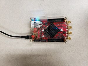
| The STEMlab 125-14 Red Pitaya board is an Field Programmable Array (FPGA) that has 2 Analog to Digital Converters (ADC) that sample data at a rate of 125 MSPS and 2 Digital to Analog Converters (DAC) that sample data at a rate of 125 MSPS. This FPGA utilizes a Xilinx Zynq 7010 System on a Chip (SoC) that has 512 MB of DDR3 random access memory. This Red Pitaya board also utilizes a dual core ARM Cortex A9 processing system. |
Laser Interferometer[edit | edit source]
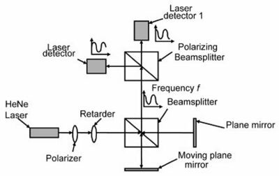
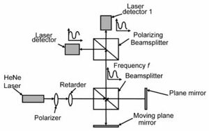
| A laser interferometer consists of two laser beams that are generated by the same source. The first beam goes through a beam expander and illuminates the target of the beam. The second beam is directed to a sensor to pick up the data. The main path depends on the main laser and how it reacts when the two beams interfere with one another producing 'spackle'. This spackled pattern is then captured and stores that data for interpretation. A laser interferometer is basically a filter that filters the spackle from the original beam to the FPGA. |
Pound-Drever-Hall Control Loop[edit | edit source]
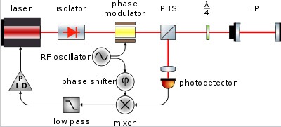
| This figure shows the Block Diagram for a generic Pound-Drever-Hall control loop. This type of a control loop is used for controlling lasers and laser like functions. This control loop is needed for high precision because all lasers have frequencies that wander. The Pound-Drever-Hall technique is used to stabilize the frequency of light being emitted by stabilizing the frequency. A laser can have instability due to temperature variations, mechanical imperfections as well as laser gain. The system takes two inputs, one is the laser beam, and one is the filtered laser beam. It then performs multiple calculations to send out a correction signal back to the laser in a continuous loop. |
Proportional-Integral-Derivative Calculation[edit | edit source]
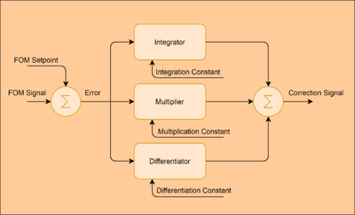
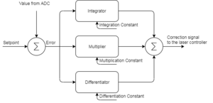
| The Proportional-Integral-Derivative calculation receives it's input from the output of the FOM calculation between the two analog inputs. These signals output an overall error from the desired value from the actual value given. This value then goes into an integrator, a multiplier, and a differentiater. These three part each have a given constant that will be applied to the input value they are given. They all output a value and then another error is calculated with these three values. This final error is then sent as a feedback control signal to the laser system. |
Deliverables[edit | edit source]
The deliverables for this project are as follows:
1. Be able to demonstrate two Red Pitaya boards communicating back and forth.
2. Be able to demonstrate the acquisition of data and the storing this data
3. Be able to gather input data from a laser
4. Be able to demonstrate the usage of a Proportional-Integral-Derivative Calculation to calculate a correction signal.
5. Be able to use the Pound-Drever-Hall loop to control the laser
Specifications[edit | edit source]
| Image | Description/Specifics |
|---|---|
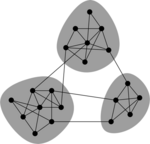
| 1. Modular design that will allow multiple implementations across multiple platforms.
2. 2 Analog-To-Digital Converter Inputs and 1 Analog-To-Digital Converter Output 3. High Speed Data Sampling -- Fastest Attainable | |
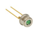
| 1. This laser diode (aka laser) that will be used will be connected to a cable, then a voltage amplifier, and then the Red Pitaya board. This is the laser diode we will be using since it is low cost and has one predominate laser light frequency instead of multiple.
2. The L850VG1 laser has an operating voltage of between 2.2 V and 2.6 V and a current of 6mA. 3. We will heat this laser up by modifying the current level or by using an outside second heating source. | |
| 1. Figure shows the basic functionality of the laser interferometer.
2. Input Sampling Rate of 10Ms/s and Input Resolution >= 16 bits 3. Control Loop Bandwidth of >= 5 kHz (Desired 10 kHz) | |
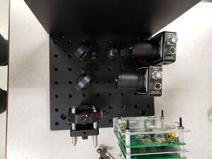
| 1. The figure shows the current setup that will be controlled by the Pound-Drever-Hall control loop. This is the base setup for the laser interferometer.
2. Input Sampling Rate of 1ks/s and Input Resolution >= 16 bits 3. Bandwidth of 100 kHz |
Design Considerations[edit | edit source]
1. Some things we will need to consider is how we will get multiple boards to communicate on a synchronized clock signal. Options involve using the clock cycle of a master board and have all the other boards synchronize to it. Or we can use SATA connectors and move resistors on the boards to use an external clock source.
2. How we will gather data and store that information. We can gather data through the analog inputs and store the data on the disk of one of the boards, or output the data to a script or file. In other words, would we rather store the data on the hardware or on the software.
3. How we will be able to create a control loop. The Red Pitaya boards allow for the use of software, hardware and a mix of the two. Some of the control loop may need to utilize a hardware description language software (like Vivado) to create a control loop and then the software to the desired specification; however, we could only need one or the other.
4. Some other things we will need to keep into consideration the input voltage and current. We need to make sure that they aren't too high due to the potential of 'burning up' the FPGA or too low causing incomplete or inaccurate readings. To do this, we will potentially be using a separate heating mechanisms for additional control and temperature measurements. With this, we will need some sort of interface to control the thermal unit.
Project Learning[edit | edit source]
The learning for this project was done around a period of about 8 weeks. In these weeks, we spent hours looking through a variety of academic journals and scientific articles. Much of our learning was spent investigating on whether or not other teams have been successful in data acquisition using FPGAs and what sort of benefits comes with using FPGAs versus other boards. The one suggested by our client to use was a board known as the Red Pitaya. The Red Pitaya has been used in data acquisition platforms before twice by two separate teams. Those teams were able to get their board working successfully and so with the glaring evidence that this is a viable solution as well as the extensive product comparison sheet, we decided to run with it.
We needed to completely understand the laser we were using and what type of voltage it needs to operate and why this laser was the best laser for our cause. We needed to know its operating range as well as frequency/wavelength range.
Some of the project learning that we completed included understanding the functionality of the Pound-Drever-Hall Loop. We needed this type of control loop due to the laser that we will be analyzing based off of the voltages given off from the photo detector the laser beam hits.
Another section of our project learning was understanding the basics of a Proportional-Integral-Derivative Calculation. This calculation will result in our correction signal and understanding what each variable does and where the value came from was pertinent to implement this system.
More research also went into how will we output data from hardware to software or using either one to store the data. Understanding the Red Pitaya Interface, the Zynq 7010 SoC, and AXI Interfaces was a very important aspect to designing a functioning system.
Finally, the last big section for project learning was finding different plans of attack for synchronizing the clocks multiple Red Pitaya boards as well as getting a time stamping capability for the data coming into the Red Pitayas.
Most of the project learning that has been done so far has been through reading papers and other sources. The Zynq Chip documentation and all Red Pitaya documentation from their sites were also major contributors to our knowledge. Most of these papers are stored in the following google drive folder:
https://drive.google.com/drive/folders/16vyaEGdfl7epmlNNZf9rPNHG0yYrHRFh
Final Design[edit | edit source]
| System Diagram | Explanation |
|---|---|
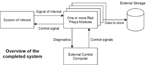
| This diagram shows the relationship between all major parts of the system. The system of interest for this project is the Laser Interferometer system but could ideally be some other system that one would want to control. From this system, a signal is sent to the input of one or more Red Pitaya Boards. The boards will send diagnostics to a computer as well as send the data being collected from the input to an external data storage that can be used later. The Red Pitaya board will take all information gathered and recalculate any changes that can be made to the input system, and then sends a feedback control signal back to the laser interferometer system. | |
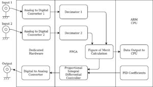
| The system itself will utilize two fast analog inputs and a singular output. Each of the two analog inputs will be decimated to 16-bits of resolution, and then compared to one another. Also, after each value goes through the decimation process, it will be sent out to the CPU before the FOM calculation. The FOM calculation will take input 2 from the second photo-detector and divide it by input 1 from photo-detector 1. The result will then be sent into the PID controller for the PID calculation. This PID calculation will send out the feedback signal that will adjust the output of the laser. | |
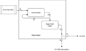
| This Red Pitaya board will use the Analog-to-Digital Converter (ADC) to take an input coming from the output of the photo-detector. This signal will be sent into an accumulator. The accumulator will accumulate 16 14-bit inputs and then average them by 16, to give us a higher resolution in total (roughly 16-bits). The output of this decorator will then be sent to a Figure-Of-Merit (FOM) calculation as well as to the CPU for users to interpret and store the data. The FOM which will compare the inputs from the second analog input and divide it by the first input to give the resulting difference. This FOM value will then be sent into the Proportional-Integral-Derivative Control Loop. | |
| The PID controller receives it's input from the output of the FOM calculation between the two analog inputs. These signals output an overall error from the desired value from the actual value given. This value then goes into an integrator, a multiplier, and a differentiater. These three part each have a given constant that will be applied to the input value they are given. They all output a value and then another error is calculated with these three values. This final error is then sent as a feedback control signal to the laser system. | |
| The hardware implementation of this project resulted in the use of a Custom IP that packaged up all of the code for getting the inputs from the ADC that are pushed through a Decimator and then it performs a Figure-of-Merit Calculation which gets pushed into the Proportional-Integral-Derivative Calculation to finally be outputted through the DAC. Then the Custom IP is imported into a new project that consists of a block diagram that interfaces with the AXI Interface that then can be pushed to the software. It will be pulled from the software by using the Zynq processing chip to hold the data coming from the AXI Stream Data FIFO. |
Validation[edit | edit source]
This section hold our teams overall plan to validate all portions of our design followed by the testing procedures for how we validated each step of our design process.
Design Validation Plan[edit | edit source]
| REQUIREMENT | TEST | TEST SUBJECT | INITIAL TARGET DATE | ADJUSTED TARGET DATE | RESULTS | RECOMMENDATION / COMMENTS | STATUS |
|---|---|---|---|---|---|---|---|
| Both boards must be able to be powered. | Ensure that the board is on when plugged into power source | Board one and board two. | Initial: 10/30/2019 | Adjusted: 11/14/2019 | Performed by John Ashby on 11/14/2019. Both boards turned on normally. | None, both boards work. | COMPLETED |
| Get both boards blink their LED's and test resting voltages. | Prove basic functionality of the boards are working as expected. | Board one and board two. | Initial: 11/06/2019 | Adjusted: 12/06/2019 | Performed by Alexis Wilson and Jared Reichle on 12/04/2019. Was able to run a python scripts built into the boards to test different functionalities the boards should be able to perform.
Performed by Alexis Wilson 12/05/2019. Testing the resting voltages given off by the slow analog inputs. |
Connect an outside source to them with a constant input to see how the voltages are being read. | COMPLETED |
| Have both boards connect to computer at same time | Create a setup that we will be able to use for control two boards at once through one machine. | Board one and board two. | Initial: 11/06/2019 | Adjusted: 12/06/2019 | Performed by Alexis Wilson and Jared Reichle on 12/04/2019. Was able to run a Python script to cause both boards to blink their LED's at the same time, however not simultaneously. | Improve this by causing both LED's to run simultaneously instead of having to run one board, then the next. | COMPLETED |
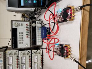
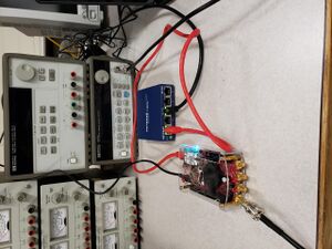
| Have board one communicate to board two. | Prove board two can receive data packages from the board one, it will respond with either an analog or digital output. | Board one and board two. | Initial: 11/06/2019 | Adjusted: 12/06/2019 | Performed by Alexis Wilson, John Ashby, and Jared Reichle on 12/05/2019. We hooked up the output of board one to the input of board two. We outputted a signal generated inside board one and used the oscilloscope inside board two to see the results coming from board two's input. | Get a dedicated SMA to SMA cable to minimize noise from one board to the other. | COMPLETED |
| Have board two communicate to board one. | Prove board one can receive data packages from the board two, it will respond with either an analog or digital output. | Board one and board two. | Initial: 11/06/2019 | Adjusted: 12/06/2019 | Performed by Alexis Wilson, John Ashby, and Jared Reichle on 12/05/2019. We hooked up the output of board two to the input of board one. We outputted a signal generated inside board two and used the oscilloscope inside board one to see the results coming from board one's input. | Get a dedicated SMA to SMA cable to minimize noise from one board to the other. | COMPLETED |
| Ensure that data collection is working on both boards | Connect a rudimentary sensor to any of the ADC connectors and read/interpret data. | Board one and board two. | Initial: 11/20/2019 | Adjusted: 12/20/2019 | Performed by Alexis Wilson and John Ashby on 12/05/2019. We were able to push a signal using a function generator to both boards individually and see the input being data being acquired. We used a graph of a signal to prove data was coming in. | Being able to store the data that is being inputted, either to the disk or to an output spreadsheet. | COMPLETED |
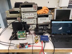
| Build the Pound-Drever-Hall loop instrument | Ensure that the laser diode, the photo-detector, and the filter (Fourier) are functioning as expected. | Measurement instrument with laser, detector, filter, all on an aluminum T-rail | Initial: 01/24/2020 | Adjusted: 02/28/2020 | Performed by Alexis Wilson and John Ashby on 03/01/2020. By the use of teamwork, we were able to get the laser path finalized and it completely locked in for the project. | System is completely ready for future testing and should not need to be adjusted in the future. | COMPLETED |
| Synchronize the two Red Pitaya boards at a single clock frequency. | Ensure that both boards can be synchronized on the same clock frequency. | Board one and board two. | Initial: 01/31/2020 | Adjusted: FUTURE WORK | NA | Through trial and error, we found that a software implementation of synchronizing multiple boards to the same clock domain is not possible. A hardware instantiation will be needed to do this. | FUTURE WORK |
| Collect data from the Laser (PDH) Instrument and perform the decimation and Figure-of-Merit Calculation. | Be able to run instrumentation as desired. | Entire System | Initial: 03/13/2020 | Adjusted: NA | Performed by Alexis Wilson on 03/07/2020. Created a hardware instantiation of the decimation process by using 16 inputs from the two Analog-Digital-Converter. Took the decimated input from the second photo-detector and divided it by the decimated input from the first photo-detector to receive the Figure-of-Merit Calculation Value. | Hook this up to the software side to see what the real-time values are. | COMPLETED |
| Create a block diagram instantiation that will output the Figure-of-Merit Calculation to the CPU | Be able to run instrumentation as desired. | Entire System | Initial: 04/15/2020 | Adjusted: 04/30/2020 | Performed by Alexis Wilson on 04/28/2020. Created a Custom IP of the Decimation and Figure-of-Merit calculation that performed a Handshake to push data from the ADC clock domain to the AXI clock domain. Created Block diagram that took the Custom IP and stored the Figure-of-Merit values into an AXI-data-stream FIFO buffer that pushed to the General Purpose I/O of the Red Pitaya. | Interface this block diagram with the software to output and store the data to an external source. | COMPLETED |
| Collect data from the Laser (PDH) Instrument and output data to external source (Software). | Be able to run instrumentation as desired. | Entire System | Initial: 03/13/2020 | Adjusted: FUTURE WORK | NA | Script to perform this is in the process, and testing. The hardware block diagram is created and can create a bit-stream (bit file) that can be pushed to the Red Pitaya and used by the Software interface. Continued work on this will be required to push the data from the hardware to the software. | FUTURE WORK |
| Create a Hardware or Software implementation of the Proportional-Integral-Derivative Calculation | See if the laser self-corrects using a variety of different inputs. | Entire System | Initial: 04/15/2020 | Adjusted: FUTURE WORK | Performed by Alexis Wilson on 04/30/2020. Created a Proportional-Integral-Derivative Calculation on the hardware interface using defined K values and the Figure-of-Merit value that outputs an error signal. | Solve for the start K values that are desirable for the system instead of the random values it has now. Integrate software into this so that the K values can be updated real time for a more accurate error and correction signal. | COMPLETED |
| Control the laser using a feedback control loop | See if the laser self-corrects using a variety of different inputs. | Entire System | Initial: 04/15/2020 | Adjusted: FUTURE WORK | NA | NA | FUTURE WORK |
Test Procedures[edit | edit source]
Here are all of the test procedures we used to test the portions of the designs and validate them. They are all built from the same template attached here: File:2020 SystemSolutions TestProcedureTemplate.pdf
| Test Setup | Test | Test Procedure |
|---|---|---|
| Ensure that the board is on when plugged into power source. | Plugged both boards in and connected to the computer. If we could use Ethernet to get into the boards and see blinking lights, the test succeeded.
Note: No procedure is needed to test this, it is done before all other tests and if no lights turn on when power is plugged in, something is wrong with the board. | |
| Get both boards to execute built-in python scripts for functionality testing. | Use python scripts built into the boards to test different functionalities the boards should be able to perform. Examples: blink LED's, testing resting voltages of system, etc. If we could run these scripts on both Red Pitaya boards and get the desired outputs, the test was a success.
File:2020 SystemSolutions BasicFunctionalityTestsDocument.pdf | |
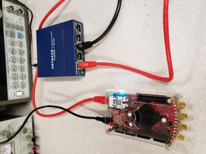
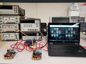
| Have both boards connect to computer at same time by creating a setup that we will be able to use for control two boards at once. | By the use of a hub/router, we hook the 2 Red Pitaya Boards to a computer through Ethernet cables. We hooked all three devices into the boards while powered on. If we could use the Ethernet connection to reach both devices, the test is a success.
Note: This test is an intermediate step for sending data packages from one board to another. | |
| Prove one board can receive data packages from the other. | Use the signal generator built into board one to generate a signal and send it as an output signal to the other board. Have the other board setup to receive a signal by using a SMA-SMA cable hooked from the first boards output to the second boards input. The second board will be set up by running it's internal Oscilloscope. If the first board is generating a signal and we can see an equivalent signal being received by the other board, then the test is a success. We can then repeat this test with the other board generating the signal and the other receiving.
File:2020 SystemSolutions MultipleBoardCommunicationTestDoc.pdf | |
| Ensure that data collection is working on both boards. | To prove data acquisition is possible, we will hook a function generator to the fast analog input of each of the board individually. On each board, one will open up the Oscilloscope and run the program. Once the measuring process is started, have input one print out the frequency and voltage of each wave. Then start the function generator, if one sees a signal as well as a frequency and a voltage, then the test is successful.
File:2020 SystemSolutions BasicDataAcquisitionTestDocument.pdf | |
| Ensure that the Pound Drever Hall Loop is functioning as expected. | After the construction of the Pound-Drever-Hall Loop instruments, we tested that the laser was able to be powered. We also checked that the laser was directed in the correct direction so that the photo-detectors could read the split beams and output the data on an Oscilloscope. | |
| Ensure that the Decimator and the Figure-Of-Merit Calculation is working on Vivado | After the code for the Decimator and Figure-Of-Merit Calculation is created, one should run a Behavioral Simulation to check that one so getting the desired outputs at the desired time. One should check for one iteration to multiple iterations to verify it is functioning as desired. | |
| Ensure that the base PID Calculation is working in Vivado. | After the code for the Proportional-Integral-Derivative Calculation is created, one should run a Behavioral Simulation to check that one so getting the desired outputs at the desired time. One should check for one iteration to multiple iterations to verify it is functioning as desired. | |
| Ensure that a hardware interface that can be interfaced with software is valid. | After the code for the project is all functioning as desire, one will package up their project into a Custom IP. Next, one will create a new project and create a block diagram that includes their Custom IP, the Processing System, and the AXI Interface. Then validate the block diagram, create the wrapper for the diagram, and go through the process of generating a bit-stream.
|
Future Work[edit | edit source]
1. Interfacing with the CPU to output the Figure of Merit calculation.
2. Interface with the CPU to store the data from the Red Pitaya.
3. Interfacing with the CPU to update the K values specified in the PID Calculation ro update real time.
4. Synchronize the clocks of multiple Red Pitaya boards.
5. Implement a time stamping system for the inputs to the system.
Note: Completing some of these steps may require editing the hardware and software that has already been created and validated.
Team Members[edit | edit source]
| Alexis Wilson
Major: Computer Engineering |
Jared Reichle
Major: Electrical Engineering | ||
| John Ashby
Major: Electrical Engineering |
Additional Documentation[edit | edit source]
This section involves any additional URL's and files that we used to design, implement, and test our projects. This includes our Project Schedule, which takes breaks into account, our Meeting Agenda and Minutes for every week, presentations done, and more.
Project Schedule:
File:2019 SystemSolutions Schedule.pdf
Meeting Agenda and Minutes:
https://drive.google.com/drive/folders/1N3VZ4ltA2Oxs-BCvWhRuyVUYpKuJwwT_
Presentations:
Snapshot 1 Presentation Work: https://drive.google.com/drive/folders/1CA4fnBwNcAqyHgFfP0Lv-MfjJVVTj_we
Preliminary Design Review: https://docs.google.com/presentation/d/1qNgygZmloFiA3YAT-jaoAQharKtmmwr0DuBmAPOwm5c/edit
Snapshot 2 Presentation: https://docs.google.com/presentation/d/1L0RskYqV3tdFSKYgVyYwhOr91OsjQqlO01ixB0C7K3Y/edit#slide=id.p
Engineering Release Review: https://docs.google.com/presentation/d/1FV5w1orSSzBVz5cCtY6RCiZNeHVd-sPDkOruZLNsGpY/edit
Snapshot 3 Presentation: https://docs.google.com/presentation/d/1QrvxnlcMGhEID9B09nCLMu37_b1lUZuZVRvd087yV3I/edit
Engineering EXPO Presentation: https://docs.google.com/presentation/d/1uLXQCIHGdgpvS2uEov06irN0FjxV3PnH-narqe_2m78/edit#slide=id.g845d0eb990_1_44
Special Thanks[edit | edit source]
We would like to give a special thank you to our sponsor Thorlabs Inc. and the team we were working with: Dr. Chris Manning, Andrew Helberts, and Mathew Philippou.
We would also like to give a special thank you to our faculty advisors Dr. Feng Li, and Dr. James Frenzel for helping us through each portion of our project.
And finally, a special thank you to all industry experts who took the time to give us insight on their knowledge and experiences.
